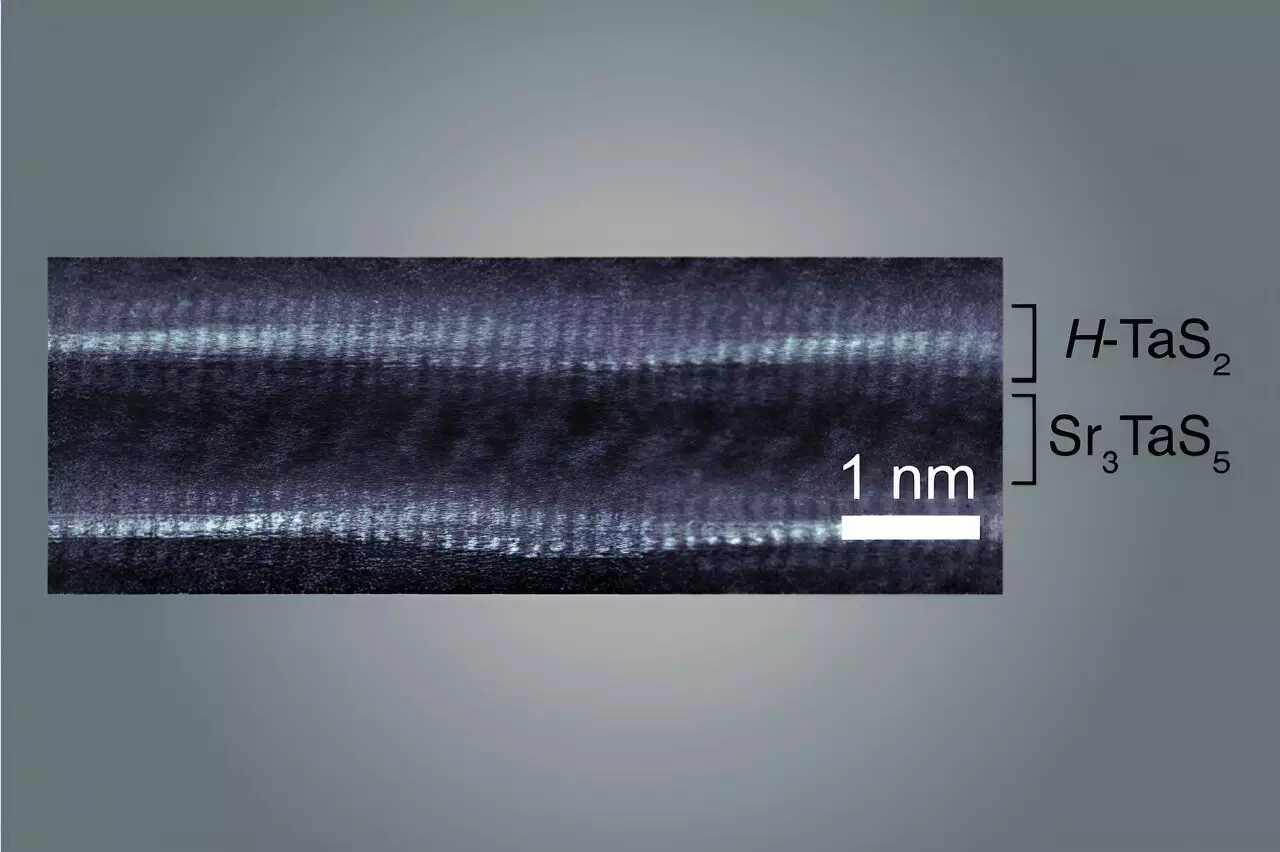
In the rapidly evolving field of material science, a team of researchers from MIT has made a remarkable breakthrough by creating a unique material showcasing unprecedented superconducting and metallic properties. The essence of their discovery lies in a novel atomic structure composed of wavy layers, each merely billionths of a meter thick. These microscopic layers can be repeatedly assembled to form macroscopically sized samples that are manageable and easier to investigate. Their findings, published in the esteemed journal *Nature*, open a plethora of possibilities for future research and practical applications in quantum physics, electronics, and beyond.
What makes this work particularly striking is the rational design approach employed by the team. Unlike traditional methods where materials are often synthesized serendipitously, the MIT researchers meticulously crafted a “recipe” based on profound insights into the chemistry and material properties of this specific class of compounds. This strategic planning gives the physicists confidence in their ability to develop additional materials that could exhibit even more extraordinary properties, underscoring a significant shift in material design philosophy.
The sheer scale of the produced samples is another noteworthy attribute of this research. By achieving materials that can be handled with the naked eye, the team has significantly alleviated the common challenges associated with studying two-dimensional materials, which are often hindered by their minuscule dimensions and complexities in assembling. The capability to explore quantum behaviors—essentially the interactions occurring at the atomic level—utilizes these large samples to investigate how specific configurations impact the material’s properties.
Joseph Checkelsky, the senior investigator and Associate Professor of Physics at MIT, emphasizes the implications of their new discovery, suggesting that the material transcends conventional definitions of a crystal. He articulates that understanding the emerging physical properties could present significant insights into the fundamental principles of quantum mechanics, which would be invaluable not only for academic pursuits but also in paving the way for innovative technologies.
The fascination with two-dimensional materials has long been amplified by phenomena like moiré superlattices—structures formed by overlaying two or more layers at slight angles. While intriguing, constructing and studying these complex structures has presented significant hurdles. The manual assembly required to create moiré materials is both labor-intensive and error-prone, often leading to inconsistencies across samples that hinder their scientific examination.
Taking a radically different approach, Checkelsky’s team has capitalized on the simplicity of creating materials through heat-based chemical reactions from powdered elements. By applying high temperatures in a controlled furnace environment, the researchers enable the natural formation of macroscopic crystals, effectively sidestepping many of the complications associated with manual assembly.
The newly discovered material consists of alternating layers of tantalum, sulfur, and spacer layers of strontium, tantalum, and sulfur, creating a structure akin to a multilayered cake. As the researchers investigated this stacking, they discovered that the unique waviness is attributed to a mismatch in the crystal lattice sizes of adjacent layers, forcing one layer to buckle to achieve alignment. This buckling phenomenon is critical for the emergence of the material’s superconducting capabilities, where electrons can flow through the material without resistance.
The team’s first author, Aravind Devarakonda, likens the behavior of these layers to paper needing to buckle to fit properly; in this scenario, aligning the different atomic layers creates conducive pathways for electron flow. The meticulously crafted wavy structure bestows upon the electrons both a preferred flow direction and variable conductivity, resulting in enhanced performance traits that could benefit numerous applications in electronics and energy systems.
As the implications of this discovery become more apparent, Devarakonda suggests that the introduction of wave structures into materials represents a pioneering exploration into uncharted territories of physics and materials science. The novelty of wavy atomic formations has hinted at potential for surprising and beneficial outcomes, embedding a sense of excitement for future innovations.
With a team composed of talented individuals from diverse institutions, including Harvard University and RIKEN in Japan, the collaboration exemplifies a multidisciplinary effort to revolutionize material design. This emerging family of materials fosters an environment ripe for exploration, pushing the boundaries of what’s possible in technological advancements by leveraging the principles of condensed matter physics.
MIT’s groundbreaking research lays a strong foundation for future endeavors in superconductivity and beyond. With confidence in their methodical design and synthesis techniques, the researchers invite the scientific community to delve into this enticing new realm, potentially leading to astonishing breakthroughs in both fundamental science and practical applications.

