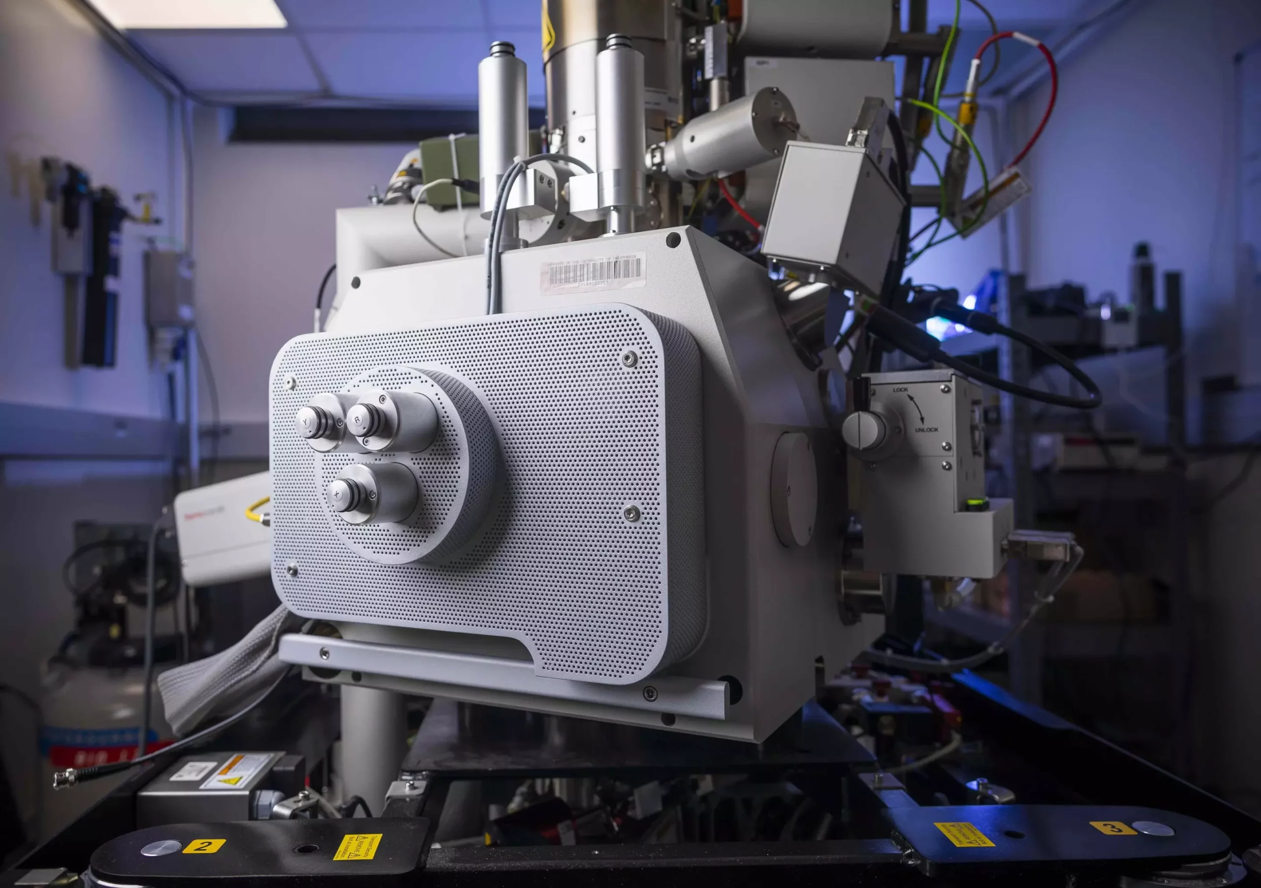
In a remarkable advancement, researchers from UC Santa Barbara have made history by creating a pioneering “movie” that captures the motion of electric charges traversing the interface of dissimilar semiconductor materials. This groundbreaking discovery employs scanning ultrafast electron microscopy (SUEM), a technique innovated in the Bolin Liao lab. For the first time, scientists have directly visualized the rapid behavior of electron movement at a heterojunction, a pivotal interface in semiconductor technology. The importance of this research lies not only in its scientific novelty but also in its potential applications across various technological domains, ranging from solar cells to high-speed electronics.
To grasp the significance of this research, one must first understand the concept of photocarriers. When sunlight strikes a semiconductor material, it excites electrons, prompting them to move. This electron movement generates an electrical current, which is harnessed for energy in devices such as solar panels. However, a major challenge arises as these photocarriers lose a majority of their energy within a staggering short time frame—on the order of picoseconds. Once viewers of this microscopic “film” see the hot carriers in action, they recognize that, although their excess energy holds great promise for energy-efficient applications, it dissipates quickly as waste heat, limiting the efficiency of contemporary photovoltaic systems.
The ability to visualize this fleeting process offers hope for better understanding and enhancing the performance of semiconductor devices. Researchers note that a thorough study of hot carriers moving through different semiconductor materials, particularly at their interfaces, is critical. Heterojunctions—a combination of two different semiconductor materials—are often where phenomena like charge carrier movement are most crucial and complex. Liao underlines the impact of this realization by highlighting that heterojunctions are integral to the functionality of a range of devices including lasers, sensors, and photocatalysis systems.
Innovating Imaging Techniques with SUEM
Bolin Liao and his research team set their sights on expanding the imaging capabilities of electron microscopes. Through the application of ultrafast laser pulses, they have effectively implemented a “picosecond-scale shutter” to synchronize an electron beam that scans across semiconductor materials. This innovative approach allows for the direct observation of hot photocarrier movement shortly after they have been excited by an optical pump beam, capturing events in a time frame that has previously been elusive to researchers.
The results of their imaging techniques proved astonishing. Instead of relying on theoretical assumptions or indirect measurements, which have historically dominated semiconductor studies, Liao’s team achieved a first-hand look at how charges behave as they transfer across the junction between two semiconductor materials—specifically, silicon and germanium. These results enable a more nuanced understanding of charge dynamics and open up avenues for refining semiconductor design.
Diving deeper into the dynamics of photocarriers reveals that upon excitation, these charges move at incredible speeds. Liao explains that when hot carriers are generated within uniform regions of silicon or germanium, they exhibit extremely high initial velocities due to their elevated temperatures. However, this phenomenon is met with a hurdle when charges are positioned near the junction. Observations indicate that a segment of these carriers becomes immobilized by the junction potential, resulting in impaired mobility.
This challenge emerges as a formidable barrier to optimizing semiconductor devices that depend on the efficient separation and collection of hot charges. The experimental confirmation of charge trapping within Si/Ge heterojunctions illustrates critical implications for semiconductor design—considerations which may warrant urgent attention from engineers and innovators in the field.
The implications of this research extend beyond mere academic curiosity. By distinctly visualizing the dynamics of hot photocarriers at heterojunctions, the team has completed a significant chapter in semiconductor research at UC Santa Barbara. The principles surrounding heterostructures, originally proposed by the esteemed late UCSB professor Herb Kroemer, are now being brought to life in ways that could redefine semiconductor practices moving forward.
This study, recently published in the Proceedings of the National Academy of Sciences, elevates the field of semiconductor physics by proving the capabilities of SUEM for realistic device studies. By grounding their findings in direct observation, researchers are not only validating theoretical models but spurring the evolution of technology that will undoubtedly influence myriad applications for years to come.

