In a groundbreaking leap forward, South Korean scientists have unlocked a new era in optical technology by mastering the mass production of quantum dot lasers. These tiny yet powerful devices are pivotal in the infrastructure of our digital world—powering data centers, enabling secure quantum communications, and connecting people across vast distances. This innovation does not merely represent an incremental step; it signifies a profound shift that could democratize access to high-performance optical components and reshape the market landscape. The implications stretch far beyond laboratory achievements, hinting at a future where cost-effective, efficient, and scalable quantum laser technology becomes the backbone of global connectivity.
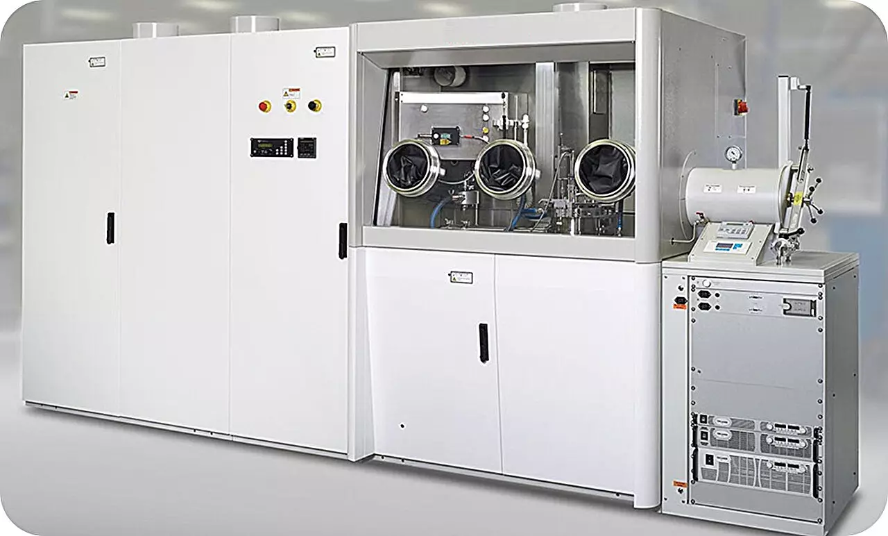
The key to this revolution lies in refining manufacturing processes—replacing traditional, slow, and expensive methods with innovative techniques capable of meeting industrial demands. Until now, the production of quantum dot laser diodes primarily depended on Molecular Beam Epitaxy (MBE), a process that, despite its precision, faced significant limitations in scalability and cost-efficiency. MBE’s slow growth rate hindered large-scale deployment, making quantum dot lasers prohibitively expensive for broader use. The South Korean research team, affiliated with the Electronics and Telecommunications Research Institute (ETRI), has turned this challenge into an opportunity by employing Metal-Organic Chemical Vapor Deposition (MOCVD), a method known for its superior throughput and scalability.
Innovative Manufacturing: A Game Changer
This technological advancement is no small feat. Developing indium arsenide/gallium arsenide (InAs/GaAs) quantum dot laser diodes on gallium arsenide substrates marks a significant milestone. The laser diodes operate efficiently within the 1.3-micron wavelength band—a critical range for optical communications, striking a balance between long-distance signal integrity and safety. By leveraging MOCVD, a process characterized by faster growth speeds and larger substrate compatibility, the team has achieved high-density, uniform quantum dot layers with impressive performance metrics.
One of the most exciting aspects of this innovation is the extended operational temperature range. The lasers demonstrated stable operation at temperatures reaching 75°C, a remarkable feat that indicates robustness suitable for real-world applications. Such thermal resilience reduces cooling requirements and increases device longevity, making these lasers viable outside of controlled laboratory environments. Moreover, transitioning from InP-based substrates—traditionally used for quantum dot lasers—to gallium arsenide substrates drastically cuts costs. InP substrates are expensive and limited in size, whereas GaAs substrates are more affordable and can be produced in larger sizes, which accelerates manufacturing efficiency.
The cost reductions are substantial. The shift to GaAs substrates, which cost less than a third of InP, coupled with the scalable MOCVD process, has the potential to drop the manufacturing costs of quantum dot lasers to less than one-sixth. This reduction is not merely a statistic but a transformative shift that could make high-quality optical communication devices accessible to a broader market. As the industry grapples with rising demand for high-speed, reliable data transmission, such cost-effective solutions are poised to fill a critical gap.
Impacts and Future Prospects
Beyond the laboratory, the industry implications are profound. The Korean research team is actively collaborating with domestic optical communication companies, sharing technology, and providing infrastructure support to facilitate commercialization. The estimated reduction in development time and production costs signifies a faster route to market, endowing local manufacturers with a competitive edge and enabling them to challenge established global players.
This innovation will likely catalyze a renaissance in South Korea’s optical component industry, fostering resilience amid global supply chain uncertainties. It empowers local companies to produce cutting-edge laser devices at a fraction of traditional costs, which can translate into cheaper consumer products, more competitive business solutions, and expanded deployment of optical networks. For society, this technological leap means faster, more reliable internet connections—whether streaming high-definition videos, managing cloud computing services, or supporting expanding smart city infrastructure.
By fundamentally altering manufacturing paradigms, this breakthrough also influences the broader field of photonics and quantum technologies. Quantum dot lasers, renowned for their temperature tolerance and substrate defect resilience, could find applications far beyond telecommunications—ranging from quantum computing to integrated photonics. South Korea’s successful demonstration underscores the importance of investment in research and development, asserting its role as a global leader driving innovation across critical sectors.
In envisioning this future, one cannot ignore the strategic importance of such advancements. They encapsulate a shift towards leveraging domestic talent and infrastructure to compete on the world stage—a move that could position South Korea not just as a technological follower but as a pioneer shaping the next generation of optical communication systems. This development exemplifies how targeted innovation, when paired with strategic investment, can unlock enormous economic and societal value, transforming the very fabric of digital connectivity in the age of quantum-enabled technologies.