In the quest for cutting-edge technology, the University of Chicago’s researchers have made remarkable strides in the understanding of antiferroelectric materials—a type of material characterized by their unique electrical properties. This particular class holds incredible promise for innovation in areas such as energy storage, sensors, and memory devices. The challenge has always been that understanding the electronic properties of these materials can be like trying to piece together a puzzle with many missing pieces. The advancements shared by Sarah King, Assistant Professor of Chemistry and lead author of a revealing study published in *Science Advances*, mark a transformation in how this intricate puzzle might be assembled.
King mentioned that their pioneering imaging technique offers unmatched spatial resolution, a capability that will undoubtedly elevate the field of material science. This newfound approach enables researchers to scrutinize the minutiae of antiferroelectric materials down to the nanoscale. Such high-resolution imaging bridges the gap in our understanding, enabling scientists to not just visualize but also manipulate the properties of these materials for specific applications. This evolution in understanding is pivotal for the rise of innovative technologies, where clarity in material properties can unlock their full potential.
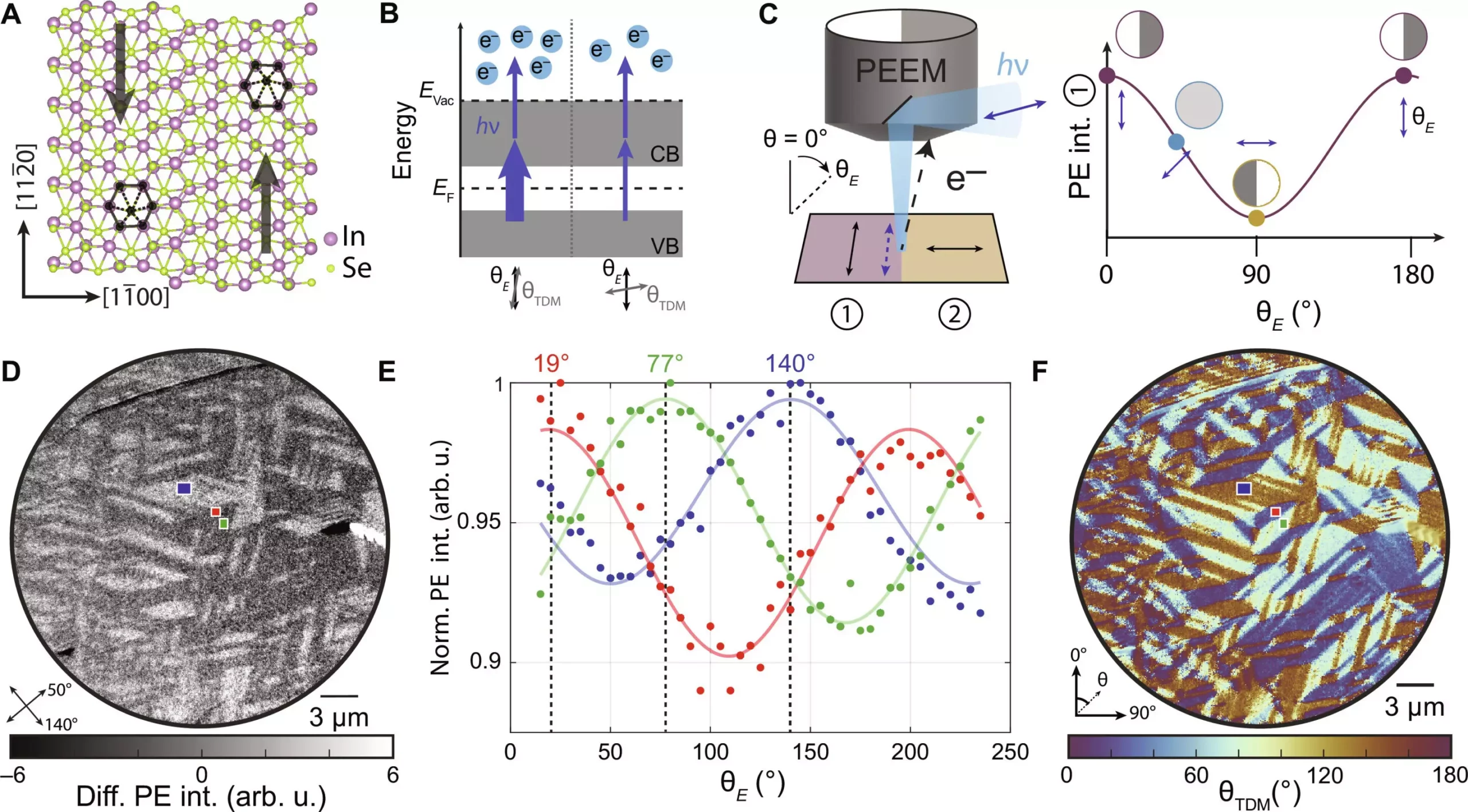
Understanding Antiferroelectricity
The core of antiferroelectric materials lies in their unique arrangement of electric dipoles. Unlike conventional ferroelectric materials that exhibit a net polarization, antiferroelectric materials maintain a delicate balance where dipoles cancel each other out. This results in no overall polarization, which provides fascinating opportunities for applications. By applying an electric field, these materials can transition to a higher energy state where polarization occurs—a characteristic that attracts attention from engineers and scientists looking for solutions in electronics and energy storage systems.
The exploration of antiferroelectric materials is not merely academic; it holds real-world implications as modern technology demands more efficient energy storage solutions. However, the challenge of characterizing these materials has often stalled progress. Traditional techniques struggle to provide the level of detail necessary to analyze these complex arrangements. Historically, a lack of resolution led scientists to speculate rather than confirm the properties of these materials.
A Breakthrough Imaging Method
In a game-changing move, King and her team utilized an advanced microscopy technique known as polarization-dependent photoemission electron microscopy. This innovative method amalgamates polarized laser light with electron imaging to not only determine electronic properties but also visualize the orientation and arrangement of dipole domains in materials like indium selenide. This level of detail was previously unfathomable, and it enables researchers to map out how these domains function and adapt under varying conditions, thereby illuminating a path for future innovations.
The implications of this breakthrough are vast. By giving scientists the tools to visualize and understand how domains interact with one another, King envisions a future where materials science can deeply examine phenomena like domain switching behaviors and phase transitions. Such insight is crucial for engineers striving to design materials that meet the specific demands of modern applications.
The Future of Antiferroelectric Materials
Moving forward, King emphasizes a keen interest in understanding the interconnectedness of various properties within materials—how they work in concert to establish ordered states. This approach transcends the simplistic view of materials as isolated entities; rather, it positions them as complex systems interlinked in their behaviors and characteristics.
With graduate students and postdoctoral researchers contributing to this research, the collaborative spirit exemplified in King’s lab underscores the importance of diverse perspectives and skills in the pursuit of scientific discovery. These promising developments not only enhance the understanding of antiferroelectric materials but also inspire a whole new generation to push the boundaries of what’s technologically possible.
These remarkable advancements in imaging techniques represent a significant leap in our ability to unlock the mysteries of antiferroelectric materials. As the field progresses, the potential applications promise to touch every aspect of our lives, from energy efficiency to the very creation of next-generation devices. The meticulous work being done at the University of Chicago demonstrates that sometimes, the key to innovation lies in our ability to see beyond what is readily visible.