Recent advancements in the field of integrated photonic circuits promise to transform both classical and quantum signal processing. A collaborative effort by scientists from the Faculty of Physics at the University of Warsaw, along with partners from Italy, Iceland, and Australia, has led to the development of perovskite crystals. These crystals, which have been engineered into precise geometries, are poised to play multifacetedroles in nonlinear photonics as components like waveguides, couplers, splitters, and modulators. The findings of this study, published in *Nature Materials*, detail the innovative fabrication techniques of these structures and highlight the groundbreaking edge lasing phenomenon, a crucial aspect of modern optical technologies.
Innovative Materials: The Role of Perovskites
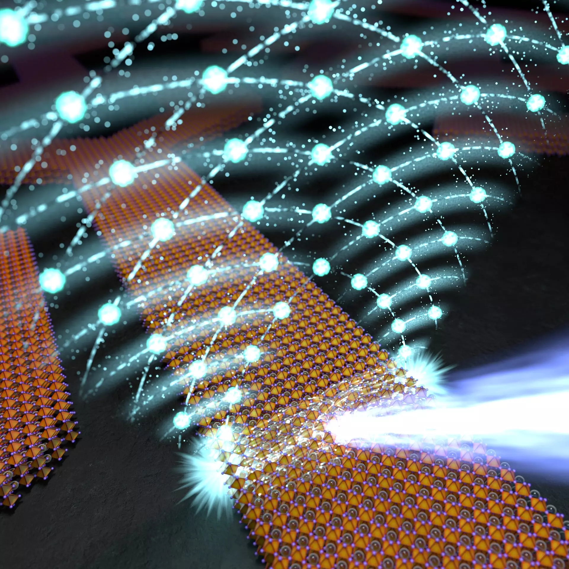
Perovskites are a class of materials known for their exceptional versatility. As explained by Professor Barbara Piętka of the University of Warsaw, perovskites can exist as polycrystalline layers, nano- and micro-crystals, or larger bulk forms. Each form has significant applications, ranging from solar cells to laser technology. The specific perovskite utilized in this research, CsPbBr3 (cesium-lead-bromide), has emerged as a particularly promising semiconductor for optical applications. Its noteworthy characteristics, such as high exciton binding energy and oscillator strength, facilitate enhanced interactions between light and matter, enabling nonlinear light amplification with reduced energy requirements. This is a game-changer for future optical devices.
To fabricate these perovskite crystals with remarkable precision, the researchers employed scalable synthesis methods. A microfluidic approach was pivotal; it allowed for the growth of crystals from a solution within narrow polymer molds, thereby permitting intricate designs to be imprinted from templates. Key to this process was maintaining controlled conditions regarding solution concentration and temperature, as well as ensuring a saturated solvent vapor atmosphere.
The groundwork laid by Anna Szerling at the Łukasiewicz Research Network illustrates the innovative use of nearly atomically smooth gallium arsenide templates crafted through advanced techniques like electron-beam lithography and plasma etching. This precision in creating high-quality single crystals has set a new standard in crystal fabrication, as researchers successfully shaped CsPbBr3 into various geometries—from sharp angles to smooth curves.
One of the standout achievements of this research is the demonstration of polaritonic lasing from the edges and corners of microwires. This phenomenon marks a departure from traditional lasing methods. According to Professor Piętka, the emitted light’s characteristics are closely tied to strong light-matter interactions, indicating the formation of a non-equilibrium Bose-Einstein condensate of exciton-polaritons. This type of lasing is unique in that it stemmed from strong coupling rather than the conventional Purcell effect.
The high coherence of the emitted light from various regions of the crystal has been confirmed through advanced spectroscopic techniques, affirming the presence of a coherent, macroscopically extended polariton condensate. Dr. Helgi Sigurðsson from the University of Iceland contributed to understanding this phenomenon, while rigorous experimental validations underscore the research team’s confidence in these groundbreaking findings.
This exploration into the nonlinear photonics of perovskite materials not only enhances academic understanding but also paves the way for innovative applications. The ability of polariton condensates to travel considerable distances within crystals suggests remarkable potentials for developing highly compact systems capable of performing both classical and quantum computing tasks on-chip. As Professor Michał Matuszewski notes, the implications of these discoveries could herald the advent of devices capable of operating at the single-photon level, thereby integrating nanolaser technology alongside waveguides for intricate, efficient systems.
In addition, the compatibility of these structures with existing silicon technology poses significant commercial advantages. The robust nature of perovskite structures and the ease of their manipulation will likely foster a new wave of optical devices that are not only efficient but also accessible for a variety of practical applications.
The synthesis and application of perovskite crystals in integrated photonic circuits represents a monumental leap for the field of nonlinear photonics. The collaborative efforts of international researchers have illuminated potential pathways that could redefine how optical technologies are utilized in the near future. As the exploration of these remarkable materials continues, we stand on the precipice of a new era in photonic innovation, where the possibilities for shaping light—and by extension, our technological capabilities—are limited only by our imagination.